14.5 SPI/I2S Interface
14.5.1 Overview
The SPI/I2S is a synchronous serial controller that can be connected to a variety of external Analog-to-Digital converters (ADC), audio and telecommunication codecs and many other devices that use serial protocols for data transfer. The SPI/I2S Controllers directly support the following protocols:
- Motorola* Serial Peripheral Interface (SPI)
- Inter-IC Sound protocol (I2S).
The SPI/I2S operates as full-duplex devices for the SPI and I2S protocols
The SPI/I2S can be configured to operate in Master mode (the attached peripheral functions as a slave) or Slave mode (the attached peripheral functions as a master). And it supports serial bit rates from 6.3 Kbps (minimum recommended speed) up to 52 Mbps. Serial data sample size can be set to 8, 16, 18, or 32 bits in length. A FIFO is provided for transmit data, and a second independent FIFO is provided for Receive data. The two FIFOs are both 32 samples deep x 32 bits wide or 64 samples deep x 16 bits wide.
The FIFOs can be loaded or emptied by CPU using programmed I/O (PIO) or DMA burst transfers.
14.5.2 Features
- Directly supports Motorola* Serial Peripheral Interface (SPI)
- The I2S is supported by programming, and data sample sizes can be set to 8, 16, 18 or 32 bits
- One FIFO for Transmit data (TXFIFO), and a second independent FIFO for Receive data (RXFIFO). For Non-Packed Data mode, the two FIFOs are each 32 rows deep x 32 bits wide for a total of 32 samples
- FIFO Packed mode allows double depth FIFOs if the samples are 8 bits or 16 bits wide. For Packed Data mode, both FIFOs are 64 locations deep x 16 bits wide for a total of 64 samples
- 52 Mbps maximum serial bit-rate
- Master mode and Slave mode operation are supported
- Receive-without-Transmit operation
- Audio clock control to provide a 4x or 8x output clock to support most standard audio frequencies
14.5.3 Functional Description
Data transfers between an SPI/I2S and memory are initiated by the CPU using programmed I/O (PIO) or DMA bursts. Separate Transmit and Receive FIFOs and serial data paths permit simultaneous transfers in both directions to and from the external peripheral, depending on the protocols chosen.
PIO can transfer data between:
- The CPU and the FIFO Data Register for the TXFIFO
- The CPU and the FIFO Data Register for the RXFIFO
- The CPU and the SPI/I2S configuration and status registers
DMA bursts can transfer data between:
- The memory and the FIFO Data Register for the TXFIFO
- The memory and the FIFO Data Register for the RXFIFO
Data written to the FIFO Data Register by either the CPU or DMA is automatically transferred to the Transmit FIFO. When reading the FIFO Data Register by either the CPU or DMA, the “oldest” data in the Receive FIFO is automatically transferred to the FIFO Data Register.
14.5.3.1 SPI/I2S FIFO Access
The data is accessed through the TXFIFO and RXFIFO. A CPU access, that is normally triggered by an interrupt caused by an SPI/I2S Status Register event, takes the form of PIO, transferring one FIFO entry per access and must always be 32-bits wide. The CPU writes to the TXFIFO are 32-bits wide, but the serializing logic ignores all bits beyond the programmed FIFO data size (see SSCR[DSS] fields in the Registers List). The CPU reads from the RXFIFO are also 32-bits wide, but the data that is received by the RXD interface signal is written, with zeroes inserted in the MSBs down to the programmed data size, into the RXFIFO.
The TXFIFO and RXFIFO can also be accessed by DMA bursts, which must be 8, 16, or 32 bytes in length, and must transfer one FIFO entry per access.
The TXFIFO and RXFIFO are each seen as one 32-bit location by the CPU. For data transmission, the SPI/I2S takes the data from the TXFIFO, serializes it, and transmits it via the output serial interface signal to the external peripheral. Data received from the external peripheral via the input interface signal is converted to parallel words and written into the RXFIFO.
A programmable FIFO trigger threshold, when exceeded, generates an interrupt or DMA service request that, if enabled, signals the CPU or DMA, respectively, to empty the RXFIFO or to refill the TXFIFO.
The TXFIFO and RXFIFO are differentiated by whether the access is a Read or a Write transfer. Reads from the FIFO Data Register automatically target the RXFIFO. Writes to the FIFO Data Register automatically target the TXFIFO. From a memory-map perspective, the TXFIFO and the RXFIFO are at the same address. Each FIFO is 32 rows deep x 32 bits wide for a total of 32 data samples. Each sample can be 8, 16, 18, or 32 bits in length.
FIFO Operation in Packed Mode
When the TXFIFO and RXFIFO are operating in packed mode, each FIFO is 64 rows deep x 16-bits wide for a total of 64 data samples. For packed mode, each sample can be 8 or 16 bits in length.
When the data is serialized and transmitted, Bits 15 to 0 are transmitted first, followed by Bits 31 to 16.
When the TXFIFO and RXFIFO are operating in packed mode, they may best be thought of as a single entry of 32 bits holding two 8- or 16-bit samples. Thus, the CPU or the DMA should write and read 32 bits of data at a time where each Write or Read transfers two samples. The entire FIFO width (32 bits) must be read/written in this mode. The SPI/I2S does not support writing two separate 16-bit samples in this mode. Calculate the thresholds based on the number of 32-bit Writes or Reads, not the number of 16-bit or less values.
Note: At serial bit rates approaching 13 MHz for continuous data transfers, the DMA might not be able to access the RXFIFO or TXFIFO fast enough to avoid overflow or underflow, respectively. Using packed mode improves performance.
14.5.3.2 Trailing Bytes in RXFIFO
When the number of samples in the RXFIFO is less than its trigger threshold level and no additional data is received, the remaining bytes are called RXFIFO trailing bytes. RXFIFO trailing bytes can be handled by either the CPU or by DMA, as indicated by the Trailing Byte field in the SSCR[TRAIL]. RXFIFO trailing bytes are identified by means of a time-out mechanism and the existence of data within the RXFIFO after timeout.
Note: When FIFO packed mode is used, the DMA can not be used to handle the RXFIFO trailing bytes. The RXFIFO trailing bytes must be handled by the CPU.
Timeout
A timeout condition exists when the RXFIFO has been idle for a period of time defined by the value programmed within the SSTO[TIMEOUT] field. When a timeout occurs, the Receiver Time-out Interrupt bit, SSSR[TINT], is set to 1, and if the Receiver Time-out Interrupt Enable bit, SSINTEN[TINTE], is set, a timeout interrupt signals the CPU that a timeout condition has occurred. The timeout timer is reset after a new data sample is received into the RXFIFO. Once the SSSR[TINT] bit is set, it must be cleared by writing 0x1 to the SSSR[TINT] bit. Clearing it also causes the timeout interrupt, if enabled, to be de-asserted.
Peripheral Trailing Byte Interrupt
It is possible for the DMA to reach the end of its Descriptor chain while removing RXFIFO data. When this happens, the CPU must take over because the DMA can no longer service the SPI/I2S until a new chain is linked. When the DMA has reached the end of its Descriptor chain with data in the RXFIFO, the SPI/I2S:
- Sets the Peripheral Trailing Byte Interrupt bit, SSSR[PINT].
- Asserts the SPI/I2S interrupt to signal to the CPU that a peripheral trailing-byte interrupt condition has occurred (if the interrupt is enabled by setting the Peripheral Trailing Byte Interrupt Enable bit, SSINTEN[PINTE]).
- Sets the End Of Chain, SSSR[EOC]. If more data is received after the SSSR[EOC] field was set (and it remains set), then the SSSR[PINT] field is set. The SSSR[EOC] field must be cleared by writing 0x1 to it.
- Once the SSSR[PINT] field is set, the CPU must clear the bit by writing 0x1 to it. Clearing it also de-asserts the SPI/I2S interrupt if it has been enabled (SSINTEN[PINTE] = 1).
The remaining bytes must then be removed with the PIO method by the CPU as described in Removing FIFO Trailing Bytes or by reprogramming a new Descriptor chain and restarting the DMA. Programmers need to be aware of this possibility. For details, refer to Section DMA about How DMA Handles Trailing Bytes.
Removing FIFO Trailing Bytes
When the Trailing Byte, SSCR[TRAIL], bit is cleared, trailing bytes left in the RXFIFO are handled by the CPU programmed I/O method. This is the default method.
If a timeout occurs, the CPU is only interrupted by a timeout interrupt if it has been enabled by setting the Receiver Time-out Interrupt Enable SSINTEN[TINTE] field. To read out the trailing bytes from the RXFIFO, software should wait for the timeout interrupt and then read all trailing bytes as indicated by the Odd Sample Status, SSSR[OSS], Receive FIFO Level, SSSR[RFL], and Receive FIFO Not Empty, SSSR[RNE] fields. To remove trailing bytes using PIO, enable the timeout interrupt by setting the SSINTEN[TINTE] field.
Note. If FIFO Packed mode is enabled (SSFCR[FPCKE]=1), trailing bytes must be removed using programmed I/O. If the SSSR[OSS] field is set, then the last FIFO line only contains one sample.
When the Trailing Byte SSCR[TRAIL] bit is set, trailing bytes left in the RXFIFO are handled by the DMA controller.
A DMA service request is issued automatically after the SSCR[TRAIL] field is set and a timeout occurs, SSSR[TINT]=1. The DMA empties the RXFIFO unless the DMA reaches the end of its Descriptor chain. When handling trailing bytes using the DMA, if a timeout occurs and the RXFIFO is empty (SSSR[RNE]=0), an end-of-receive (EOR) is sent to the DMA.
If a DMA EOC occurs (SSSR[EOC]=1) at the time that the last sample is read out of the RXFIFO (the DMA Descriptor chain was just exactly long enough) and the timeout counter is still running (that is, a timeout has not occurred and SSTO[TIMEOUT] is non-zero), then, when the timeout does occur, the SPI/I2S generates a DMA request. When this occurs, re-initialize the DMA registers and re-enable the channel for the SPI/I2S to send its EOR to the DMA controller.
Notes.
- When the SPI/I2S is running in Network mode and the FIFO Packing Enable SSFCR[FPCKE] bit is set, use the CPU to handle trailing bytes in the RXFIFO with the SSCR[TRAIL] bit cleared and the SSINTEN[PINTE] bit set. After the Peripheral Trailing Byte Interrupt SSSR[PINT]=1 occurs, the interrupt service routine must clear the SSNWC[MOD] bit and wait for SSNWS[NMBSY] bit to go low before removing any extra or trailing samples from the RXFIFO, which can be discarded.
- When the SSNWC[MOD] bit is set, the SPI/I2S continues transceiving data even after the TXFIFO is empty and until the SSNWC[MOD] bit is cleared. Since the DMA does not have a way to clear the SSNWC[MOD] bit, it is possible that extra samples are received in the RXFIFO. Since software must clear the SSNWC[MOD] bit, the CPU must also handle the trailing bytes.
14.5.3.3 Data Formats
The types of formats used to transfer serial data between the CPU and external peripherals are described in the following subsections.
Serial Data Formats for Transfer to/from Peripherals
Two interface signals for each SPI/I2S transfer data between the CPU and external peripherals. Although serial-data formats exist, each has the same basic structure, and in all cases, the interface signals used are:
- SS_SCLK - Defines the bit rate at which serial data is driven onto and sampled from the port
- SS_FRM - Defines the boundaries of a basic data “unit” which is comprised of multiple serial bits
- SS_TX - The serial datapath for transmitted data from the SPI/I2S to the peripheral
- SS_RX - The serial datapath for received data from peripheral to the SPI/I2S
A data frame can contain 8, 16, 18, or 32 bits (SSCR[DSS] fields. Serial data is transmitted with the MSb first. The formats directly supported are the Motorola* SPI, and the I2S protocol is supported by programming the PSP format.
The SS_FRM function and use varies between each format. SS_FRM is programmable in direction, delay, polarity, and width. Both Master and Slave modes are supported.
- SPI format: SS_FRM functions as a chip select to enable the external device (target of the transfer) and is held active-low during the data transfer. During continuous transfers, the SS_FRM signal can be either held low or pulsed depending upon the value of the Motorola* SPI SS_SCLK phase setting in SSCR[SPH], Master and Slave modes are supported. SPI is a full-duplex format.
- PSP format (I2S): SS_FRM is programmable in direction, delay, polarity, and width. Master and Slave modes are supported. PSP can be programmed to be either full- or half-duplex format. I2S is supported by programming PSP format.
The SS_SCLK function and use varies between each format:
- SPI format: Programmers choose which edge of SS_SCLK to use for switching Transmit data and for sampling Receive data. In addition, moving the phase of SS_SCLK can be user-initiated, shifting its active state one-half cycle earlier or later at the start and end of a frame. Master and Slave modes are supported, and in both, the SS_SCLK only toggles during active transfers (does not run continuously).
- PSP format (I2S): Programmers choose which edge of SS_SCLK to use for switching Transmit data and for sampling Receive data. In addition, programmers can control the Idle state for SS_SCLK and the number of active clocks that precede and follow the data transmission. Master and Slave modes are supported. When driven by the SPI/I2S port, the SS_SCLK toggles only during active transfers, not continuously. When the SS_SCLK is driven by another device, it is allowed to be either continuous or driven only during transfers, but certain restrictions on PSP parameters apply.
Normally, if the serial clock (SS_SCLK) is driven by the SPI/I2S port, it toggles only while an active data transfer is underway. However, there are several conditions that may cause the clock to run continuously. If the Receive-without-Transmit mode is enabled by setting the Receive Without Transmit, SSRWT[RWOT], the SS_SCLK toggles regardless of whether Transmit data exists within the Transmit FIFO. The SS_SCLK also toggles continuously if the SPI/I2S port is in Network mode. At other times, SS_SCLK is held in an inactive or idle state, as defined by the specified protocol under which it operates.
Motorola* SPI Format
The SPI format has four possible sub-modes depending on the SS_SCLK edges selected for driving data and sampling received data and on the selection of the phase mode of SS_SCLK for a complete description of each sub-mode).
Note. The following description applies only when SPH = 0 and SPO = 0. Other combinations of SPH and SPO result in different polarities and timings.
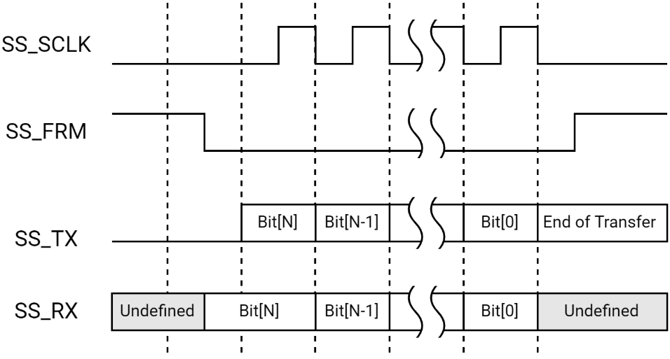
When the SPI/I2S is disabled or in idle mode, SS_SCLK and SS_TX are low and SS_FRM is high. When Transmit data is ready to be sent, SS_FRM goes low (one clock period before the first rising edge of SS_SCLK) and stays low for the remainder of the frame. The most significant bit of the serial data is driven onto SS_TX one half-cycle later. Halfway into the first bit period, SS_SCLK asserts high and continues toggling for the remaining data bits. Data transitions on the falling edge of SS_SCLK and is sampled on the rising edge of SS_SCLK. 8, 16, 18, or 32 bits can be transferred per frame.
With the assertion of SS_FRM, Receive data is driven simultaneously from the peripheral on SS_RX , MSb first. Data transitions on SS_SCLK falling edges and is sampled by the controller on SS_SCLK rising edges. At the end of the frame, SS_FRM is de-asserted high one clock period (one half clock cycle after the last falling edge of SS_SCLK) after the last bit has been latched at its destination and the completed incoming word is shifted into the “incoming” FIFO. The peripheral can drive SS_RX to a high-impedance state after sending the last bit of the frame.
SS_TX retains the last value transmitted when the controller goes into Idle mode, unless the SPI/I2S is disabled or reset (which forces SS_TX to zero).
For back-to-back transfers, start and completion are like those of a single transfer, but SS_FRM does not de-assert between words. Both transmitter and receiver are configured for the word length and internally track the start and end of frames. There are no “dead” bits; the LSb of one frame is followed immediately by the MSb of the next.
When in Motorola* SPI format, the SPI/I2S can be either a master or a slave device, but the clock and frame direction must be the same. For example, the Serial Bit Rate Clock Direction, SSCR[SCLKDIR], and the Frame Direction, SSCR[SFRMDIR], fields must either both be set or cleared.
When in Motorola* SPI format, if the SPI/I2S is the master and SSPSP[ETDS] is cleared, the end-of-transfer data state for SS_TX is low. If the SPI/I2S is the master and SSPSP[ETDS] is set, the end-of-transfer data state for SS_TX remains at the last bit transmitted (LSb). If the SPI/I2S is the slave, then the SSPSP[ETDS] is undefined. SS_RX is undefined before the frame is active and after the LSb is received. SS_RX must not float. When the SPI/I2S is configured as a master and SSCR[TTE] is set, SSPSP[ETDS] is ignored and SS_TX becomes high impedance between active transfers.
Below are depicted the four possible configurations for the Motorola* SPI frame protocol for a single transmitted frame.
Instead, below is depicted how back-to-back frames are transmitted for the Motorola* SPI frame protocol.
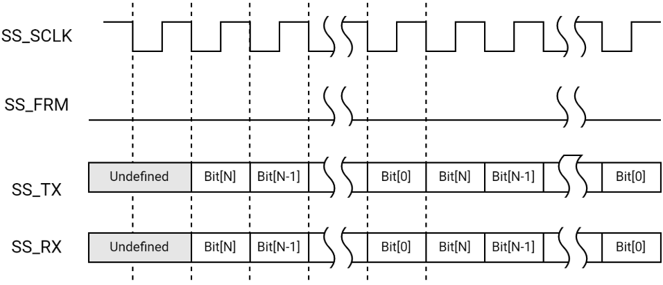
Note. The phase and polarity of SS_SCLK can be configured for four different modes. This example shows just one of those modes (SSCR[SPO] and SSCR[SPH] cleared). Other settings for SPO and SPH result in different polarities and timing.
Programmable Serial Protocol (I2S) Format
The PSP format defines programmable parameters that determine the transfer timings between data samples and used for I2S protocol.
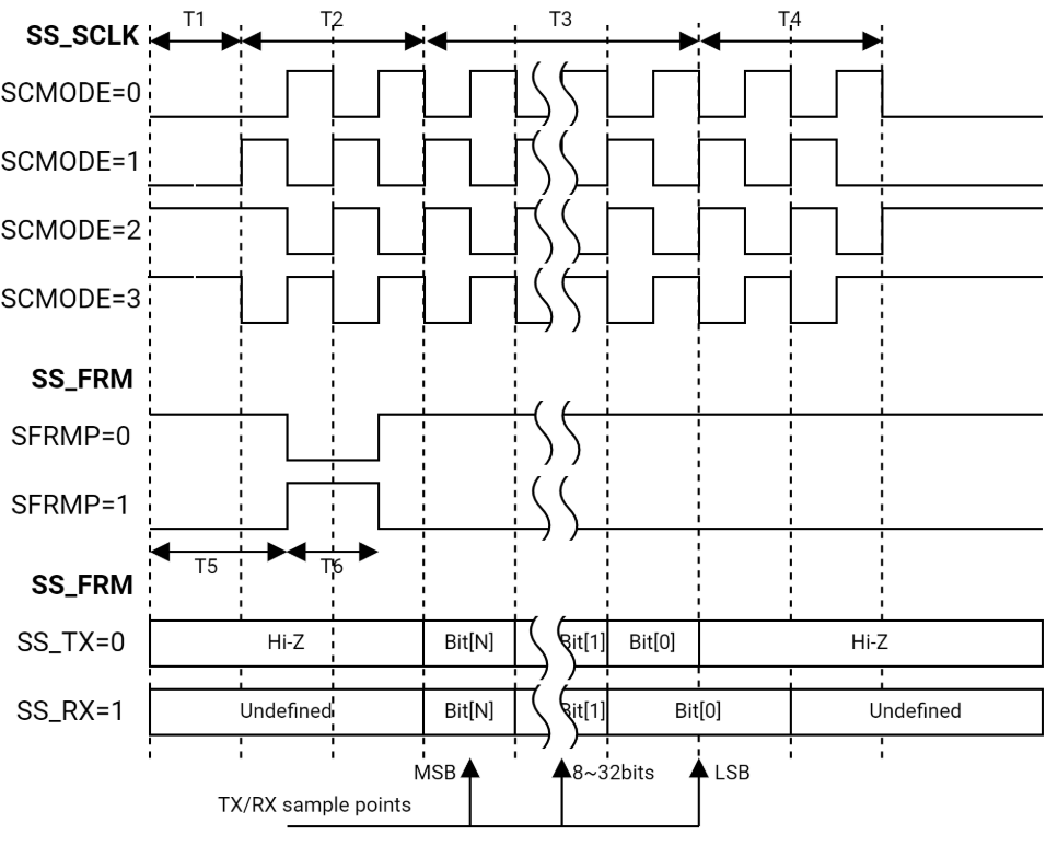
Four serial clock modes are defined in the Serial Bit-rate Clock Mode, SSPSP[SCMODE]. These modes select the SS_SCLK rising and falling edges for driving data, sampling received data, and the SS_SCLK idle state.
The Idle and Disabled modes of the SS_TX, SS_SCLK, and SS_FRM interface signals are programmable using the following fields in the SSPSP Register: End Of Transfer Data State (SSPSP[ETDS]), Serial Frame Polarity (SSPSP[SFRMP]), and Serial Bit-rate Clock Mode (SSPSP[SCMODE]). When transmit data is ready, SS_SCLK remains in its idle state for the number of serial clocks (SS_SCLK) periods programmed into the Start Delay (SSPSP[STRTDLY]) field in the SSP Programmable Serial Protocol Register.
SS_SCLK then starts toggling. SS_TX remains in the idle state for the number of serial clock periods programmed into the Dummy Start (SSPSP[DMYSTRT]) field. SS_FRM is asserted after the number of half serial clock periods programmed into the Serial Frame Delay (SSPSP[SFRMDLY]) field. SS_FRM remains asserted for the number of serial clock periods programmed into the Serial Frame Width (SSPSP[SFRMWDTH]) field, then SS_FRM de-asserts.
Serial data of 8, 16, 18, or 32 bits can be transferred per frame by setting the SSCR[DSS] fields to the preferred data size select. Once the last bit (LSb) is transferred, SS_SCLK continues toggling for the number of serial clock periods programmed into the Dummy Stop (SSPSP[DMYSTOP]) field. Depending on the value programmed into the End Of Transfer Data State (SSPSP[EDTS]) field when the SPI/I2S port goes into idle mode, SS_TX either retains the last bit-value transmitted or is forced to 0 unless the SPI/I2S port is disabled or reset, which forces SS_TX to 0.
With the assertion of SS_FRM, Receive data is driven simultaneously from the peripheral onto SS_RX, MSb first. Data transitions on the SS_SCLK edge based on the serial-clock mode that is selected (SSPSP[SCMODE]) and is sampled by the SPI/I2S port on the opposite clock edge. When the SPI/I2S port is a master to SS_FRM and a slave to SS_SCLK, at least three extra SS_SCLKs are needed at the beginning and end of each block of transfers to synchronize control signals from the APB clock domain into the SPI/I2S clock domain (a block of transfers is a group of back-to-back continuous transfers).
In general, because of the programmable nature of the PSP protocol, this protocol can be used to achieve a variety of serial protocols, including I2S.
The programmable protocol parameters of SPI/I2S are tabled below.
| Symbol | Definition | Range | Units |
|---|---|---|---|
| - | Serial clock mode (SSPSP[SCMODE]) 0 = Fall, rise, low 1 = Rise, fall, low 2 = Rise, fall, high 3 = Fall, rise, high | (Drive, Sample, SS_SCLK Idle) | - |
| - | Serial frame polarity (SSPSP[SFRMP]) | High or low | - |
| T1 | Start delay (SSPSP[STRTDLY]) | 0 to 7 | Clock period |
| T2 | Dummy start (SSPSP[EDMYSTRT] + SSPSP[DMYSTRT]) | 0 to 15 | Clock period |
| T3 | Data size (SSCR[DSS]) | 4 to 32 | Clock period |
| T4 | Dummy stop (SSPSP[EDMYSTOP] + SSPSP[DMYSTOP]) | 0 to 31 | Clock period |
| T5 | SS_FRM delay (SSPSP[SFRMDLY]) | 0 to 127 | Half-clock period |
| T6 | SS_FRM width (SSPSP[SFRMWDTH]) | 1 to 63 | Clock period |
| - | End of transfer data state (SSPSP[ETDS]) | Low or bit 0 | - |
The SS_FRM delay (T5) must not extend beyond the end of T4. The SS_FRM width (T6) must be asserted for at least one SS_SCLK period and should be de-asserted before the end of T4 (for example, in terms of time, not bit values
- (T5 + T6) <= (T1 + T2 + T3 + T4)
- 1<= T6 < (T2 + T3 + T4)
- (T5 + T6) >= (T1 + 1)
to ensure that SS_FRM is asserted for at least two edges of SS_SCLK). Program T1 to 0 when SS_SCLK is enabled by the SSCR[SCFR] fields.
While the SPI/I2S can be programmed to generate the assertion of SS_FRM during the middle of the data transfer (for example, after the MSb has been sent), the SPI/I2S port is unable to Receive data in frame-Slave mode. Transmit data transitions from the end-of-transfer-data state (SSPSP[ETDS]) to the next MSb data value upon assertion of the internal version of SS_FRM. Program the SSPSP[STRTDLY] field to 0x00 whenever SS_SCLK or SS_FRM is configured as an input (for example, SSCR[SCLKDIR] and SSCR[SFRMDIR] are cleared).
Note. When the SPI/I2S port is slave to the frame, the sum of T1+T2+T3+T4 can be less than the actual time from the beginning of the current frame to the beginning of the next frame. For example, when the rate of SS_SCLK is 12.8 MHz and the data sample size is 16-bits, the beginning of the frame can occur at a rate of 8 kHz.
14.5.3.4 High Impedance on SS_TX
The SPI/I2S supports placing the SS_TX into high impedance during idle time instead of driving SS_TX as controlled by the TXD Three-State Enable (SSCR[TTE]) and TXD Three-state Enable On Last Phase (SSCR[TTELP]) field. The SSCR[TTE] enables a high-impedance state on SS_TX. The SSCR[TTELP] determines on which SS_SCLK phase SS_TX becomes high impedance.
Motorola* SPI Format
For Motorola* SPI format, SSCR[TTELP] must be cleared. If SSCR[TTE] = 1. SS_TX functionality is depicted below.
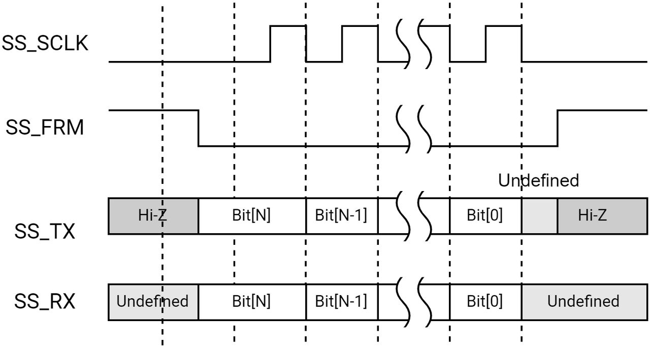
For Motorola* SPI format, SS_TX goes to a high-impedance state whenever SS_FRM is not asserted.
PSP Format
SS_TX functionality when SSCR[TTE] = 1, SS_SSCR[TTELP] = 0 and SSCR[SFRMDIR] = 1, are depicted below.
14.5.3.5 Network Mode Operation
The SSNWC[MOD] bit selects between Normal and Network modes. Normal mode (MOD = 0x0) is used when using the Motorola* Serial Peripheral Interface (SPI). Network mode (MOD = 0x1) is used for the I2S protocol.
Software should set MOD only when using the PSP format. If the SPI/I2S port is a master of the clock and SSCR[SCLKDIR] is cleared, then setting MOD causes the SS_SCLK to run continuously.
When in Network mode, only one SS_FRM is sent (Master mode) or received (Slave mode) for the number of time slots programmed into the SSNWC[FRDC] field. When beginning in Network mode, while the SPI/I2S port is a master to the SS_FRM interface signal, the first SS_FRM signal does not occur until after data is in the TXFIFO. After assertion of the first SS_FRM signal, if the SPI/I2S port is a master to SS_FRM, subsequent SS_FRM signals continue to assert regardless of whether data resides in the TXFIFO. Therefore, the transmit underrun bit, SSSR[TUR], is set to 1 if there is no data in the TXFIFO and the SPI/I2S port is programmed to drive SS_TX data in the current time slot, even if the SPI/I2S port is master to SS_FRM. When using PSP format in Network mode, the parameters SFRMDLY, STRTDLY, DMYSTOP, DMYSTRT must all be 0. The other parameters SFRMP, SCMODE, FSRT, SFRMWDTH are programmable.
When the SPI/I2S port is a master to the SS_FRM signal and a need arises to exit from Network mode, software should:
- Clear the SSNWC[MOD] bit. SSCR[SSE] does not need to change
- Wait until SSNWS[NMBSY] is cleared
- Disable the SPI/I2S port by clearing SSCR[SSE]
- Before exiting Network mode, verify the TXFIFO is empty (SSSR[TFL]=0 and SSSR[TNF]=1)
- If data remains in the TXFIFO after the Network mode is exited, a non-Network mode frame is sent
Due to synchronization delay between the internal bus and the SPI/I2S port clock domain, one extra frame may be transmitted after software clears the SSNWC[MOD] bit. The SPI/I2S port continues to drive SS_SCLK (if SSCR[SCLKDIR] is cleared) and SS_FRM (if SSCR[SFRMDIR] is cleared) until the end of the last valid time slot.
If the SPI/I2S port is a slave to both SS_SCLK (SSCR[SCLKDIR] set) and SS_FRM (SSCR[SFMRDIR] set), the SSNWS[NMBSY] bit remains asserted until the SSNWC[MOD] bit is cleared or until one SS_SCLK after the end of the last valid time slot.
14.5.3.6 Parallel Data Formats for FIFO Storage
All CPU and DMA accesses transfer one FIFO entry per access. Data in the FIFOs is either stored with one 32-bit value per data sample (in non-packed or sample > 16 bits) or in a 16-bit value in packed mode when the data is 4 or 16 bits. Within each 32- or 16-bit field, the stored data sample is right-justified, with the LSb of the word in bit 0. In the Receive FIFO, unused bits are packed as zeroes above the MSb. In the Transmit FIFO, unused “don’t-care” bits are above the MSb. For example, DMA and CPU accesses do not have to write to the unused bit locations. Logic in the SPI/I2S automatically formats data in the Transmit FIFO so that the sample is properly transmitted on SS_TX in the selected frame format.
14.5.3.7 FIFO Operation
This section describes the operation of Transmit and Receive FIFOs.
Two separate and independent FIFOs are present for transmitting (TXFIFO to peripheral) and receiving (RXFIFO from peripheral) serial data. The FIFOs are filled or emptied by programmed I/O or DMA bursts.
Using Programmed I/O Data Transfers
FIFO filling and emptying can be performed by the CPU in response to an interrupt from the FIFO logic. Each FIFO has a programmable FIFO trigger threshold that triggers an interrupt. When the number of entries in the RXFIFO exceeds the RXFIFO Trigger Threshold (SSFCR[RFT]) field, an interrupt is generated (if enabled) that signals the CPU to empty the RXFIFO. When the number of entries in the TXFIFO is less than or equal to the TXFIFO Trigger Threshold (SSFCR[TFT]) field plus 1, an interrupt is generated (if enabled) that signals the CPU to refill the TXFIFO.
The SSSR can be polled to determine how many samples are in a FIFO and whether the FIFO is full or empty. Software is responsible for ensuring that the proper RXFIFO Trigger Threshold and TXFIFO Trigger Threshold values are chosen to prevent Receive FIFO Overrun and Transmit FIFO Underrun error conditions.
Using DMA Data Transfers
The DMA controller can also be programmed to transfer data to and from the FIFOs. To prevent overruns of the TXFIFO or underruns of the RXFIFO when using the DMA, be careful when setting the FIFO trigger threshold levels by setting the correct DMA burst sizes. TXFIFO overruns and RXFIFO underruns are silent errors: There is no indication of the overrun or underrun condition other than missing data at the receiving end of the link. The DMA burst size must be smaller than the trigger threshold.
The programming model for using DMA is:
- Program the total number of transmit/receive byte lengths, burst sizes, and peripheral width.
- When not using the FIFO packed mode, program the Width field in the DMA Command Registers to 0x1 for FIFO data sizes of 8 bits, 0x2 for FIFO data sizes of 16 bits, and 0x3 for FIFO data sizes of more than 16 bits. When not using packed mode, the SPI/I2S stores one data sample per FIFO location where each FIFO has 16 locations. For example, the DMA burst size must not exceed 16 bytes when Width field in the DMA Command Registers is set to 0x1 (byte wide).
- When using FIFO packed mode, program the Width field in the DMA Command Registers to 0x3. When using packed mode, the SPI/I2S stores two data samples per FIFO location where each FIFO has 16 locations. Therefore, the DMA burst size must not exceed 16 bytes when Width field in the DMA Command Registers is set to 0x3 (more than 16 bits wide).
- Because the SPI/I2S is not flow-controlled and has only 16 location FIFOs, software must program the TXFIFO threshold (SSFCR[TFT]) field, RXFIFO threshold (SSFCR[RFT]) field, and the DMA burst size to ensure that a TXFIFO overrun or RXFIFO underrun does not occur. Software must also ensure that the SPI/I2S DMA requests are properly prioritized in the system to prevent overruns and underruns.
- Program the preferred values into the SSCR
- Enable the SPI/I2S by setting the Synchronous Serial Port Enable (SSCR[SSE]) field
- Set the run bits in the DMA Command Register
- The DMA waits for either the TXFIFO or RXFIFO service request
- If the receive byte length is not an even multiple of the transfer burst size, a trailing-byte condition may occur
In full-duplex formats where the SPI/I2S always receives the same number of data samples that it transmits, the DMA channel should be set up to transmit and receive the same number of bytes.
Note. When the FIFO Packing Enable (SSFCR[FPCKE]) field is set to 0x1, the SSFCR[TFT] and SSFCR[RFT] fields represent twice the number of FIFO entries as when the packing enable bit is 0x0. So, when in packed mode, the maximum allowed DMA burst size (8 or 16) could be doubled.
14.5.3.8 Baud-Rate Generation
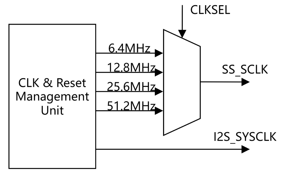
When the SPI/I2S is configured as the master (output) of SS_SCLK as determined by clearing the SSCR[SCLKDIR] field, the baud rate (or serial bit-rate clock SS_SCLK) is obtained by selecting from one of the four fixed clock sources (6.4 MHz, 12.8 MHz, 25.6 MHz, or 51.2 MHz). A variable clock source is available from the output of two dithering dividers external to the SPI/I2S unit. Clock selection is achieved by writing to the Functional Clock Select field of the SPI/I2S Clock/Reset Control Register.
When the source clock is to be changed, software must:
-
Disable the SPI/I2S port by writing 0x0 to SSCR[SSE]
-
Disable the SPI/I2S port internal clock by clearing the appropriate bit in the Clock Enable Register
-
Write clock and reset related registers to enable functional clocks to the SPI/I2S units
-
If applicable, set appropriate values for the frequency dividers
-
Enable APB clock to the SPI/I2S unit
-
Set the SSCR[SSE] bit to re-enable the SPI/I2S port. Whenever the baud rate is to be changed, software must:
- Disable the SPI/I2S port by clearing SSCR[SSE] bit
- Set the SSCR[SSE] bit to re-enable the SPI/I2S port
Wait two SS_SCLK cycles before writing new data to the TXFIFO. The SPI/I2S Baud Rate Generation is depicted below.
14.5.4 Register Description
Note. The base address of SPI/I2S registers are tabled below.
| Register Name | Address |
|---|---|
| SHUB_SSP0_BASE | 0xC0885000 |
| SSP3_BASE | 0xD401C000 |
| SSPA0_BASE | 0xD4026000 |
| SSPA1_BASE | 0xD4026800 |
| SSP2_BASE | 0xF0613000 |
SSCR REGISTER
SPI/I2S top control register. Offset: 0x0
| Bits | Field | Type | Reset | Description |
|---|---|---|---|---|
| 31:19 | RSVD | RO | 0x0 | Reserved for future use |
| 18 | TTELP | RW | 0x0 | TXD Three-state Enable On Last Phase 0 = SS_TX is three-stated 1/2 clock cycle after the beginning of the LSb 1 = SS_TX output signal is three-stated on the clock edge that ends the LSb |
| 17 | TTE | RW | 0x0 | TXD Three-State Enable 0 = SS_TX output signal is not three-stated 1 = SS_TX is three-stated when not transmitting data |
| 16 | SCFR | RW | 0x0 | Slave Clock Free Running 0 = Clock input to SS_CLK is continuously running 1 = Clock input to SS_CLK is only active during data transfers. |
| 15 | IFS | RW | 0x0 | Invert Frame Signal 0 = SS_FRM polarity is determined by the PSP polarity bits 1 = SS_FRM will be inverted from normal-SS_FRM (as defined by the PSP polarity bits). (Works in all frame formats: SPI and PSP) |
| 14 | HOLD_FRAME_LOW | RW | 0x0 | Hold Frame Low Control 1 = After this field is set to 1 and the SPI/I2S is operating in master mode. Used for SPI Format Rx FIFO Auto Full Control, which makes the frame clock is still low during there's no bit clock, or the data transfers before the stop clock will be discarded. |
| 13 | TRAIL | RW | 0x0 | Trailing Byte 0 = Trailing bytes are handled by the CPU 1 = Trailing bytes are handled by DMA bursts |
| 12 | LBM | RW | 0x0 | Loopback Mode (Test Mode Bit) 0 = Normal serial port operation is enabled 1 = Output of TX serial shifter is internally connected to input of RX serial shifter |
| 11 | SPH | RW | 0x0 | Motorola SPI SS_SCLK phase setting 0 = SS_SCLK is inactive until one cycle after the start of a frame and active until 1/2 cycle before the end of a frame 1 = SS_SCLK is inactive until 1/2 cycle after the start of a frame and active until one cycle before the end of a frame |
| 10 | SPO | RW | 0x0 | Motorola SPI SS_SCLK Polarity Setting 0 = The inactive or idle state of SS_SCLK is low 1 = The inactive or idle state of SS_SCLK is high |
| 9:5 | DSS | RW | 0x0 | SPI/I2S Work data size. Register bits value 0 |
| 4 | SFRMDIR | RW | 0x0 | SS_FRM Direction 0 = Master mode, SPI/I2S port drives SS_FRM 1 = Slave mode, SPI/I2S port receives SS_FRM |
| 3 | SCLKDIR | RW | 0x0 | SS_SCLK Direction 0 = Master mode, SPI/I2S port drives SS_SCLK 1 = Slave mode, SPI/I2S port receives SS_SCLK |
| 2:1 | FRF | RW | 0x0 | Frame Format 2'h0 : Motorola* Serial Peripheral Interface (SPI) 2'h3 : Programmable Serial Protocol (PSP) Others : reserved |
| 0 | SSE | RW | 0x0 | SPI/I2S Enable 0 = SPI/I2S port is disabled 1 = SPI/I2S port is enabled |
SSFCR REGISTER
SPI/I2S FIFO control register. Offset: 0x4
| Bits | Field | Type | Reset | Description |
|---|---|---|---|---|
| 31:22 | RSVD | RO | 0x0 | Reserved for future use |
| 21 | RXENDIAN | RW | 0x0 | Select the big endian or little endian for RX transfer 0 = big endian 1 = little endian |
| 20 | TXENDIAN | RW | 0x0 | Select the big endian or little endian for TX transfer 0 = big endian 1 = little endian |
| 19 | STRF | RW | 0x0 | Select FIFO For Test Mode Bit 0 = TXFIFO is selected for both writes and reads through the SPI/I2S Data Register 1 = RXFIFO is selected for both writes and reads through the SPI/I2S Data Register |
| 18 | EFWR | RW | 0x0 | Enable FIFO Write/read (Test Mode Bit) 0 = FIFO write/read special function is disabled 1 = FIFO write/read special function is enabled |
| 17 | RXFIFO_AUTO_FULL_CTRL | RW | 0x0 | Rx FIFO Auto Full Control After this field is set to 1 and the SPI/I2S is operating in master mode, the SS_FSM returns to IDLE state and stops the SS_SCLK. When Rx FIFO is full, the SS_FSM continues transferring data after the Rx FIFO is not full. This field is used to avoid an Rx FIFO overrun issue. 1 = Enable Rx FIFO auto full control 0 = Disable Rx FIFO auto full control |
| 16 | FPCKE | RW | 0x0 | FIFO Packing Enable 0 = FIFO packing mode disabled 1 = FIFO packing mode enabled |
| 15:14 | TXFIFO_WR_ENDIAN | RW | 0x0 | apb_pwdata Write to Tx FIFO Endian ## 2'h0 : txfifo_wdata[31:0] = apb_pwdata[31:0] ## 2'h1 : txfifo_wdata[31:0] = {apb_pwdata[15:0], apb_pwdata[31:16]} ## 2'h2 : txfifo_wdata[31:0] = {apb_pwdata[7:0], apb_pwdata[15:8], apb_pwdata[23:16], apb_pwdata[31:24]} ## 2'h3 : txfifo_wdata[31:0] = {apb_pwdata[23:16], apb_pwdata[31:24], apb_pwdata[7:0], apb_pwdata[15:8]} |
| 13:12 | RXFIFO_RD_ENDIAN | RW | 0x0 | apb_prdata Read from Rx FIFO Endian 2'h0 : apb_prdata[31:0] = rxfifo_wdata[31:0] 2'h1 : apb_prdata[31:0] = {rxfifo_wdata[15:0], rxfifo_wdata[31:16]} 2'h2 : apb_prdata[31:0] = {rxfifo_wdata[7:0], rxfifo_wdata[15:8], rxfifo_wdata[23:16], rxfifo_wdata[31:24]} 2'h3 : apb_prdata[31:0] = {rxfifo_wdata[23:16], rxfifo_wdata[31:24], rxfifo_wdata[7:0], rxfifo_wdata[15:8]} |
| 11 | RSRE | RW | 0x0 | Receive Service Request Enable 0 = DMA service request is disabled 1 = DMA service request is enabled |
| 10 | TSRE | RW | 0x0 | Transmit Service Request Enable 0 = DMA service request is disabled 1 = DMA service request is enabled |
| 9:5 | RFT | RW | 0x0 | RXFIFO Trigger Threshold This field sets the threshold level at which RXFIFO asserts interrupt. The level should be set to the preferred threshold value minus 1. |
| 4:0 | TFT | RW | 0x0 | TXFIFO Trigger Threshold This field sets the threshold level at which TXFIFO asserts interrupt. The level should be set to the preferred threshold value minus 1. |
SSINTEN REGISTER
SPI/I2S interrupt enable register. Offset: 0x8
| Bits | Field | Type | Reset | Description |
|---|---|---|---|---|
| 31:7 | RSVD | RO | 0x0 | Reserved for future use |
| 6 | EBCEI | RW | 0x0 | Enable Bit Count Error Interrupt 0 = Interrupt due to a bit count error is disabled 1 = Interrupt due to a bit count error is enabled |
| 5 | TIM | RW | 0x1 | Transmit FIFO Underrun Interrupt Mask 0 = TUR events generate an interrupt 1 = TUR events do NOT generate an interrupt |
| 4 | RIM | RW | 0x1 | Receive FIFO Overrun Interrupt Mask 0 = ROR events generate an interrupt 1 = ROR events do NOT generate an interrupt |
| 3 | TIE | RW | 0x0 | Transmit FIFO Interrupt Enable 0 = TXFIFO threshold-level-reached interrupt is disabled 1 = TXFIFO threshold-level-reached interrupt is enabled |
| 2 | RIE | RW | 0x0 | Receive FIFO Interrupt Enable 0 = RXFIFO threshold-level-reached interrupt is disabled 1 = RXFIFO threshold-level-reached interrupt is enabled |
| 1 | TINTE | RW | 0x0 | Receiver Time-out Interrupt Enable 0 = Receiver time-out interrupt is disabled 1 = Receiver time-out interrupt is enabled |
| 0 | PINTE | RW | 0x0 | Peripheral Trailing Byte Interrupt Enable 0 = Peripheral trailing byte interrupt is disabled 1 = Peripheral trailing byte interrupt is enabled |
SSTO REGISTER
SPI/I2S time out register. These registers specify the timeout (TIMEOUT) value used to signal a period of inactivity within the RXFIFO. When a timeout occurs, the SSSR[TINT] field is set. When the TIMEOUT value is set to 0x000000, no timeout occurs and the SSSR[TINT] field is not set. The TIMEOUT interval is given by the calculation in the TIMEOUT Interval Equation.
TimeOut Interval = SSTO [TIMEOUT] / APB Clock Frequency, APB Clock Frequency = 25.6 MHz OR 51.2MHz.
Offset: 0xC
| Bits | Field | Type | Reset | Description |
|---|---|---|---|---|
| 31:24 | RSVD | RO | 0x0 | Reserved for future use |
| 23:0 | TIMEOUT | RW | 0x0 | Timeout Value TIMEOUT value is the value that defines the time-out interval. The time-out interval is given by the equation shown in the TIMEOUT Interval Equation. |
SSDATR REGISTER
SPI/I2S data register. Offset: 0x10
| Bits | Field | Type | Reset | Description |
|---|---|---|---|---|
| 31:0 | DATA | RW | 0x0 | DATA This field is used for data to be written to the TXFIFO or read from the RXFIFO. |
SSSR REGISTER
SPI/I2S status register. Offset: 0x14
| Bits | Field | Type | Reset | Description |
|---|---|---|---|---|
| 31:24 | RSVD | RO | 0x0 | Reserved for future use |
| 23 | OSS | RO | 0x0 | Odd Sample Status 0 = RxFIFO entry has two samples 1 = RxFIFO entry has one sample Note: This bit needs to be looked at only when FIFO Packing is enabled (SSFCR[FPCKE] field is set). Otherwise, this bit is zero. When SPI/I2S port is in Packed mode and the CPU is used instead of DMA to read the RxFIFO, the CPU should make sure that SSSR[RNE] = 1 AND this field = 0 before it attempts to read the RxFIFO. |
| 22 | TX_OSS | RO | 0x0 | TX FIFO Odd Sample Status 0 = TxFIFO entry has an even number of samples 1 = TxFIFO entry has an odd number of samples Note: This bit needs to be read only when FIFO Packing is enabled (SSFCR[FPCKE] field is set). Otherwise, this bit is zero. |
| 21 | BCE | RW1C | 0x0 | Bit Count Error 0 = The SPI/I2S port has not experienced a bit count error 1 = The SS_FRM signal was asserted when the bit counter was not zero |
| 20 | ROR | RW1C | 0x0 | Receive FIFO Overrun 0 = RXFIFO has not experienced an overrun 1 = Attempted data write to full RXFIFO, causes an interrupt request |
| 19:15 | RFL | RO | 0x1F | Receive FIFO Level This field is the number of entries minus one in RXFIFO. When the value 0x1F is read, the RXFIFO is either empty or full, and software should read the SSSR[RNE] field. |
| 14 | RNE | RO | 0x0 | Receive FIFO Not Empty 0 = RXFIFO is empty 1 = RXFIFO is not empty |
| 13 | RFS | RO | 0x0 | Receive FIFO Service Request 0 = RXFIFO level is at or below RFT threshold (RFT) or SPI/I2S port is disabled 1 = RXFIFO level exceeds RFT threshold (RFT), causes an interrupt request |
| 12 | TUR | RW1C | 0x0 | Transmit FIFO Underrun 0 = The TXFIFO has not experienced an underrun 1 = A read from the TXFIFO was attempted when the TXFIFO was empty, causing an interrupt if it is enabled |
| 11:7 | TFL | RO | 0x0 | Transmit FIFO Level This field is the number of entries in TXFIFO. When the value 0x0 is read, the TXFIFO is either empty or full, and software should read the SSSR[TNF] field. |
| 6 | TNF | RO | 0x1 | Transmit FIFO Not Full 0 = TXFIFO is full 1 = TXFIFO is not full |
| 5 | TFS | RO | 0x0 | Transmit FIFO Service Request 0 = TX FIFO level exceeds the TFT threshold (TFT + 1) or SPI/I2S port disabled 1 = TXFIFO level is at or below TFT threshold (TFT + 1), causes an interrupt request |
| 4 | EOC | RW1C | 0x0 | End Of Chain 0 = DMA has not signaled an end of chain condition 1 = DMA has signaled an end of chain condition |
| 3 | TINT | RW1C | 0x0 | Receiver Time-out Interrupt 0 = No receiver time-out is pending 1 = Receiver time-out pending, causes an interrupt request |
| 2 | PINT | RW1C | 0x0 | Peripheral Trailing Byte Interrupt 0 = No peripheral trailing byte interrupt is pending 1 = Peripheral trailing byte interrupt is pending |
| 1 | CSS | RO | 0x0 | Clock Synchronization Status 0 = The SPI/I2S port is ready for slave clock operations 1 = The SPI/I2S port is currently busy synchronizing slave mode signals |
| 0 | BSY | RO | 0x0 | SPI/I2S Busy 0 = SPI/I2S port is idle or disabled 1 = SPI/I2S port is currently transmitting or receiving framed data |
SSPSP REGISTER
SPI/I2S programmable serial protocol control register. Offset: 0x18
| Bits | Field | Type | Reset | Description |
|---|---|---|---|---|
| 31:30 | RSVD | RO | 0x0 | Reserved for future use |
| 29:27 | EDMYSTOP | RW | 0x0 | Extended Dummy Stop Most-significant bits of the dummy stop delay. Do not use in PSP Network mode. |
| 26:25 | DMYSTOP | RW | 0x0 | Dummy Stop Least-significant bits of the dummy stop delay. Programmed value of SSPSP[EDMYSTOP] + this field specifies the number (0-31) of active clocks (SS_SCLK) that follow the end of the transmitted data. Do not use in PSP Network mode. |
| 24:23 | EDMYSTRT | RW | 0x0 | Extended Dummy Start Most-significant bits of the dummy start delay. Do not use in PSP Network mode. |
| 22:21 | DMYSTRT | RW | 0x0 | Dummy Start Least-significant bits of the dummy start delay. Programmed value of this field specifies the number (0-15) of active clocks (SS_SCLK) between the end of start delay and when the most-significant bit of transmit/receive data is driven. Do not use in PSP Network mode. |
| 20:18 | STRTDLY | RW | 0x0 | Start Delay Programmed value specifies the number (0-7) of non-active clocks (SS_SCLK) that define the duration of idle time. Do not use in PSP Network mode. |
| 17:12 | SFRMWDTH | RW | 0x0 | Serial Frame Width Least-significant bits of the serial frame width. Programmed value of this field specifies the frame width from 0x00 (one SS_SCLK cycle) to 0x3F (63 SS_SCLK cycles). |
| 11:5 | SFRMDLY | RW | 0x0 | Serial Frame Delay Programmed value specifies the number (0-127) of active one-half clocks (SS_SCLK) asserted from the most-significant bit of TX (output) or RX (input) being driven to SS_FRM. Do not use in PSP Network mode. |
| 4 | SFRMP | RW | 0x0 | Serial Frame Polarity 0 = SS_FRM is active low 1 = SS_FRM is active high |
| 3 | FSRT | RW | 0x0 | Frame Sync Relative Timing Bit 0 = Next frame is asserted after the end of the DMTSTOP timing 1 = Next frame is asserted with the LSb of the previous frame |
| 2 | ETDS | RW | 0x0 | End Of Transfer Data State 0 = Low 1 = Last Value <Bit 0> |
| 1:0 | SCMODE | RW | 0x0 | Serial Bit-rate Clock Mode 2'h0 : Data Driven (Falling), Data Sampled (Rising), Idle State (Low) 2'h1 : Data Driven (Rising), Data Sampled (Falling), Idle State (Low) 2'h2 : Data Driven (Rising), Data Sampled (Falling), Idle State (High) 2'h3 : Data Driven (Falling), Data Sampled (Rising), Idle State (High) |
SSNWCR REGISTER
SPI/I2S network control register. Offset: 0x1C
| Bits | Field | Type | Reset | Description |
|---|---|---|---|---|
| 31:20 | RSVD | RO | 0x0 | Reserved for future use |
| 19:12 | RTSA | RW | 0x0 | RX Time Slot Active, only used in network mode 0 = SPI/I2S port does not receive data in this time slot 1 = SPI/I2S port receives data in this time slot |
| 11:4 | TTSA | RW | 0x0 | TX Time Slot Active, only used in network mode 0 = SPI/I2S port does NOT transmit data in this time slot 1 = SPI/I2S port does transmit data in this time slot |
| 3:1 | FRDC | RW | 0x0 | Frame Rate Divider Control Value of 0x0-0x7 specifies the number of time slots per frame when in network mode (the actual number of time slots is this field + 1, so 1 to 8 time slots can be specified). |
| 0 | MOD | RW | 0x0 | Mode 0 = Normal mode 1 = Network mode. When setting this bit to 1, must make sure at the same time SSCR[FRF] = 0x3 |
SSNWS REGISTER
SPI/I2S network status register. Offset: 0x20
| Bits | Field | Type | Reset | Description |
|---|---|---|---|---|
| 31:4 | RSVD | RO | 0x0 | Reserved for future use |
| 3 | NMBSY | RO | 0x0 | Network Mode Busy 0 = SPI/I2S port is in network mode and no frame is currently active 1 = SPI/I2S port is in network mode and a frame is currently active |
| 2:0 | TSS | RO | 0x0 | Time Slot Status Value indicates which time slot is currently active. Because of synchronization between the SPI/I2S port's SS_SCLK domain and an internal bus clock domain, the value in this field becomes stable between the beginning and end of the currently active time slot. |
SSRWT REGISTER
SPI/I2S root control register. Offset: 0x24
| Bits | Field | Type | Reset | Description |
|---|---|---|---|---|
| 31:5 | RSVD | RO | 0x0 | Reserved for future use |
| 4 | MASK_RWOT_LAST_SAMPLE | RW | 0x0 | Mask last_sample_flag in RWOT Mode 1 = Mask 0 = Unmask |
| 3 | CLR_RWOT_CYCLE | RW | 0x0 | Clear Internal rwot_counter This field clears the rwot_counter to 0. This field is self-cleared after SSCR[SSE] = 1. 1 = Clear rwot_counter |
| 2 | SET_RWOT_CYCLE | RW | 0x0 | Set RWOT Cycle This field is used to set the value of the RWTC register to the internal rwot_counter. This field is self-cleared after SSCR[SSE] = 1. 1 = Set rwot_counter |
| 1 | CYCLE_RWOT_EN | RW | 0x0 | Enable RWOT Cycle Counter Mode 1 = Enable 0 = Disable |
| 0 | RWOT | RW | 0x0 | Receive Without Transmit 0 = Transmit/receive mode 1 = Receive without transmit mode |
SSRWTCC REGISTER
SPI/I2S root counter cycles match register.
Offset: 0x28
| Bits | Field | Type | Reset | Description |
|---|---|---|---|---|
| 31:0 | SSRWOTCCM | R/W | 0x0 | It's just total SS_SCLK Cycles The value of this register defines the total number of SS_SCLK cycles when SSP works in master and RWOT mode. When the rwot_counter matches this value, SSP returns to IDLE state and does not output SS_SCLK anymore. |
SSRWTCV REGISTER
SPI/I2S root counter value write for read request register. Offset: 0x2C
| Bits | Field | Type | Reset | Description |
|---|---|---|---|---|
| 31:0 | SSRWOTCVWR | RW | 0x0 | This register prevents the risk of instability on rwot_counter value reading, it's only valid after SPI/I2S has been enabled. Write 0 = No effect Write 1 = Capture value of rwot_counter Read = Returns the captured value of rwot_counter |